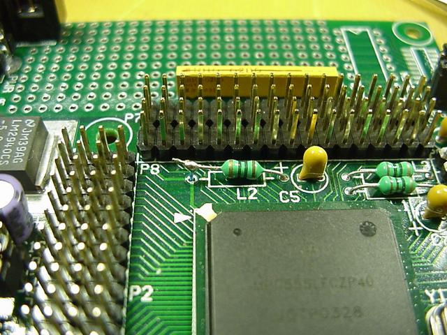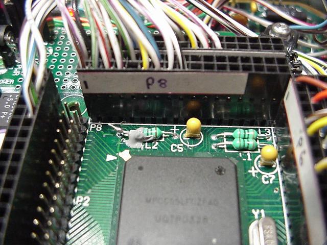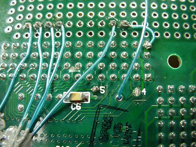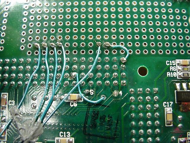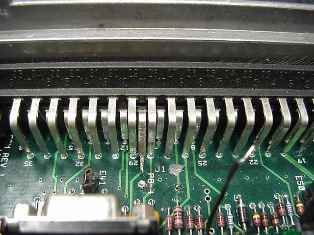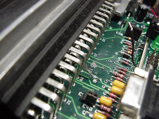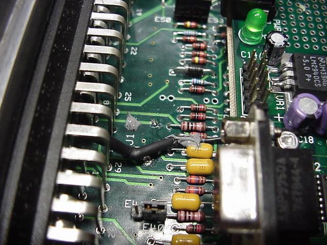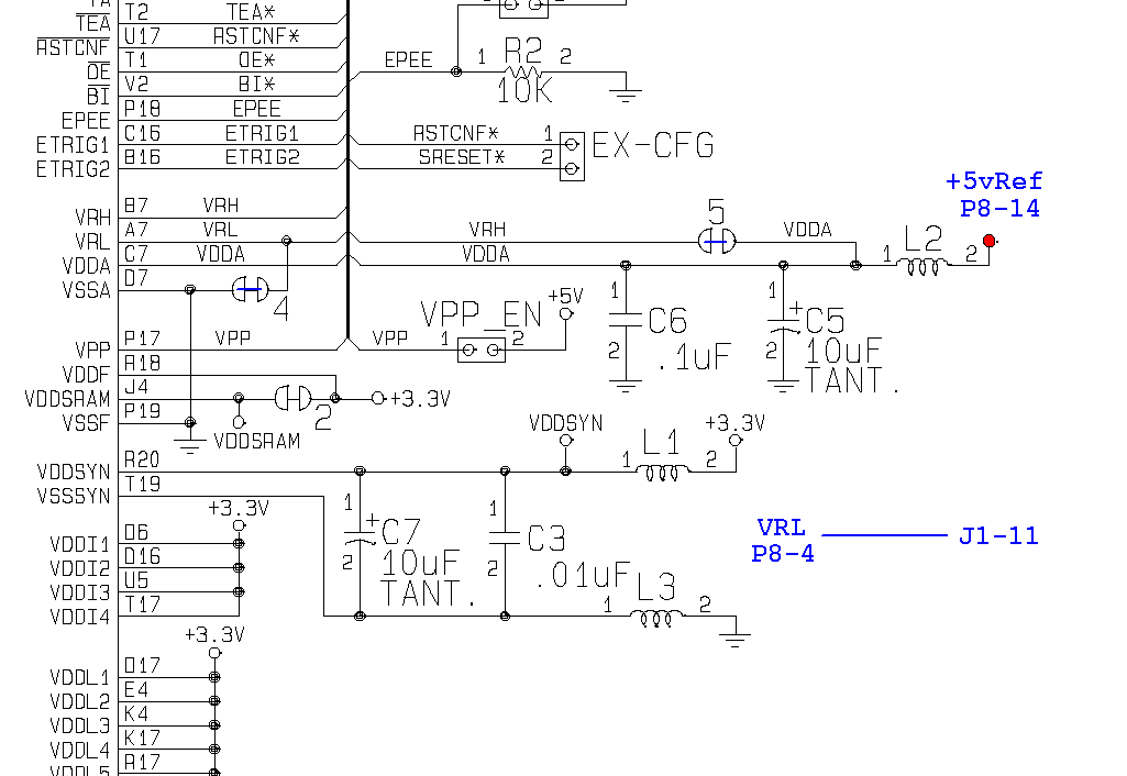
Been fighting a nasty jitter in the ADC system. It had manifested itself as an instability in the ADC readings. A one count bounce, which is approximately 5mv, could be considered acceptable. But what we were getting was a constant 1 bit jitter with many 2 to 3 bit jumps. Occasionally more. The Axiom board by itself outside of the ECM did much better than that. In fact there is an ADC test mode where the ADC input is attached to an internal divider across the VRH and VRL pins. This was very unstable in the system and rock solid by itself. It has taken quite a bit of investigating trying to determine where it was coming from. Was it a noisy reference? Noisy input signals? I changed how the ADC was powered slightly. Originally the ADC was powered by the +5VF supply and the upper reference (VRH) from the precision +5 volts. I lifted one side of L2 that was tied to the +5VF and ran it to P8-14 where the +5V reference was fed in. Of coarse it didn't fix the excessive jitter. Finally I was able to trace it down. What I had done was to taken the low side of the ADC reference (VRL) and connected to J1-11 which is the main input connector pin that is the Analog Return line back to the ECM. At this point it was tied to the common analog ground plane. This should have directed any current in the in the Analog Return line back to the low side of the ADC. Well it must have created a ground loop somewhere. Still not clear where all the current is going but I know what I needed to do to fix it. Tied the ADC's VRL (reference low side) to the low side of the ADC power supply (this was a cut pad #4 on the Axiom PCB) and brought the Analog Return from J1-11 to this junction. Now there is a random 1 bit jitter with a very rare 2 bit jumps.