+5 volt Reference Resolution
As previously discussed we have had some reservations with the +5 volt precision reference. Current limiting and protection of its
components being one and it coming up before the +5VF supply was another. Several possible resolutions were tried and would have addressed these issues
but the fact that two independent supplies where being fed into a very expensive IC, the MPC555, and numerous extra components that would have had to be butched in another
approach was settled upon. Make both the +5VF and
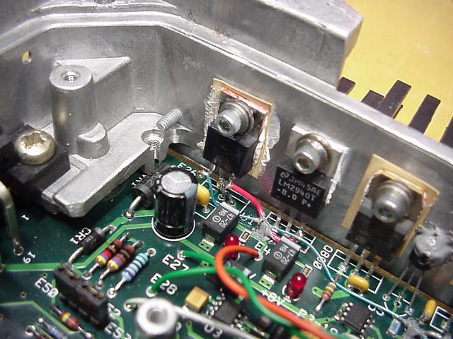
the +5VRef supplies virtually one and the same. By removing the U1, the original LM2940-5 regulator, and replacing the TO-92 (Q1) with a high power TO-220 PNP
transistor to handle the power requirements of both supplies we could then guarantee that the +5VF supply was always the same or higher than the +5VRef supply and
could use the LM2940-8 (+8VF supply) current limiting capabilities to protect from a dead short. This new TO-220 transistor was mounted in the old U1 +5VF
regulator position. By attaching it to the case we now have our thermal path. I used a 200uh toroid inductor to connect the two supplies together. This
gave a little more isolation between the dirty +5VF supply and the reference. I used a toroid because its large wire gave us a small DC resistance and a high
inductance. Need the low DC resistance so if for some reason larges amount of current were being drawn from the reference the +5VF supply would not get too
high. This could happen because the LT1021 senses on the +5VRef side of the coil.
Update (3/30/05):
Well it looks like the inductor between the two power supplies was not as good idea as it originally seemed. It did isolate the
dirty +5VF supply from the +5 volt reference but it caused a resonance. Looking at the current being drawn by the unit it was clear something wasn't
right. Large current swings were observed that where in sync with how fast the ADC was being read and whose amplitude varied by what the ADC was
reading. Really strange looking. It looks like as small current changes on the +5 volt reference caused huge current swings on the +5VF
supply. Directly connecting the two supplies eliminated this problem.

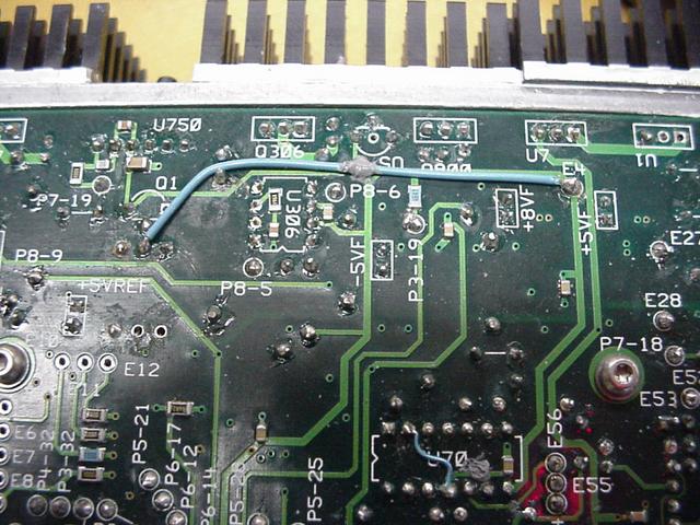
This is the new Block A Power supply schematic.
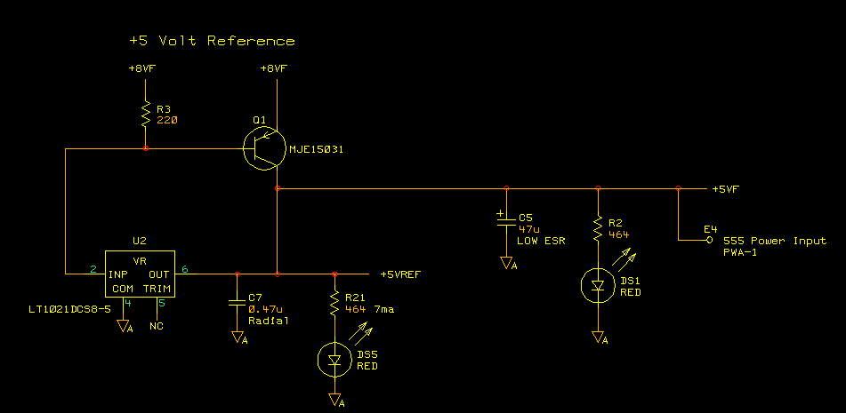
A little more clearer as to what was done.
Removed the original current limiting resistors (R4 and R8) and the small TO-92 boost transistor (Q1). The inductor was located into the
two free pads, Q1-C and the emitter side of R8. Don't forget to install the small wire into Q1-B before gluing in place.
Update (03/30/05): The inductor does not need to be loaded!
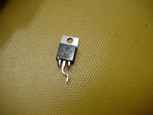
Prepare the MJE-15031 transistor by forming the leads as indicated. Never bend a lead of a TO-220 transistor without a small needle noise
pliers between the bend and the body of the transistor!
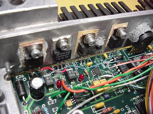
Mount the new boost transistor in the original +5VF regulator position. The tab is not grounded so assure proper isolation. Connect
its emitter to the +8FV supply, its collector will fit into old U1-3 pad, and the base is routed to the original Q1-B pad.
Tie the two supplies together on the bottom side. Jumper between the +5VF supply at E4 and the emitter side of R4. This will pick
up the decoupling inductor.
Update (03/30/05): Ignore this step!
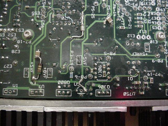
Update (03/30/05): Tie the supplies together (jumper near U5).