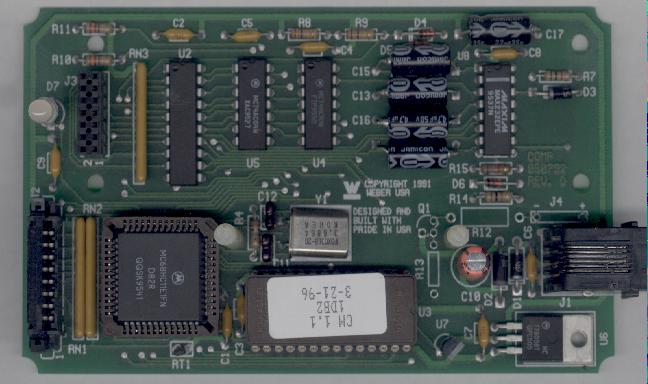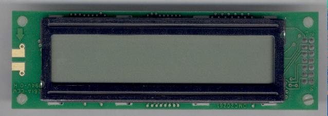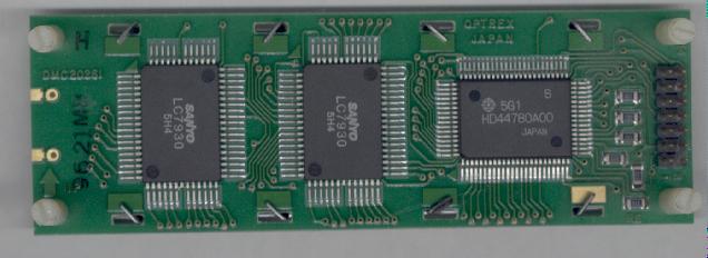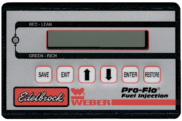
Well this is what the Edelbrock controller looks like. From this nifty 5 1/2"x3 1/2" unit you can program all the parameters of the PRO-FLO's EFI system. It uses a scrolling window system to page though all of the menus and display windows. The OPTREX DMC20261A-CEM (20 characters x 2 lines) LCD temperature compensated display brings the information to you. The display is not backlit so it can not been seen at night. Not a real smart idea to messing with at night anyhow. The buttons are a membrane type. For the most part they work well but at times they do bounce or skip a depression. As time goes along these type of buttons can become problematic. This unit communicates to the main ECU through a two wire serial interface running at 9600 baud. There are no hardwired handshaking lines used. At 9600 baud framing errors and buffer under/over runs are not a large problem so rarely is there any kind of communication errors. The data sent back and forth is checksumed by a simple byte addition routine. The PCB, which is made in the USA by WEBER USA, is well laid out and of high quality. Through hole technology throughout except for the 52 pin PLCC MC68HC11E1 socketed microprocessor. The programmable EPROM is a AM27C128 (16 Kbyte) unit. Power is supplied from the main ECU unit and regulated to +5 volts. A MAXIM MAX232EPE serial transceiver is the interface to the outside world. It contains two charge pump supplies that are capable of delivering +/- 10 volts. Only the -10 volt supply is used. The serial paths from each MPU is a little non standard. Usually there is only one signal inversion between the MPU/UART and the outside connector, usually supplied by the RS232 driver. In this system there are four more inverters in the chain. This probably came about because of a need to communicate with the ECU which looks to be a production unit that is used in Europe. If you want to connect into this serial stream with another device, say your laptop, you will need to construct an interface cable that inverts these signal lines. The rest of the circuitry is pretty straight forward digital design. The only other item of interest is the thermistor and MPU controlled -5 volt supply driving the display. This variable supply is used to compensate the LCD display for temperature variations. It uses one of the MPU's timers (OC3), which is duty cycled modulated, to generate this supply through the RS232 driver. The output of this supply is then scaled and fed back to one of the MPU's ADCs (AN1) for monitoring. It looks like the original intent was to measure the ambient temperature using the thermistor, determine the optimum Vee supply for the display section, and then adjust the duty cycle of the timer while monitoring the output voltage with the ADC. It looks like it didn't work out they way they planed for some reason. The ADC feed back is not implemented in the firmware. All it does is have one break point and two fixed timing periods. Don't know why they didn't close the loop here. It might be that they were trying to save ROM space. There is only about 60 bytes free out of the 16k ROM. The unit is wired so that it will accept a 27C256 (32 Kbyte) ROM but maybe cost considerations verses display performance dictated the direction they went. You can check out the pdf schematic here. Some of the parts have Data Sheets. Below are a couple of pictures of its internals....