RE2 - v2+ GPSDO & 10 MHz Disciplined Frequency Reference
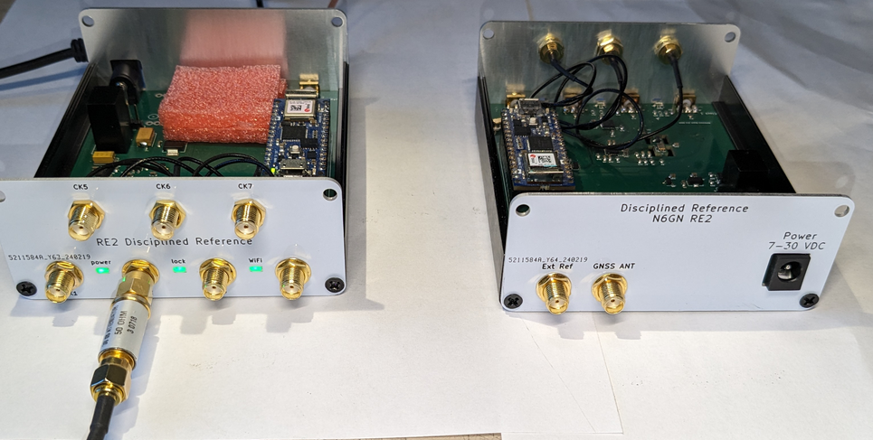
From the original RE to the latest version, these
disciplined REferences have had the primary objective to be
very low cost, accurate and high value devices for
synchronizing amateur radio communications equipment. LF
through VHF communications by way of the ionosphere has been a
particular target. Design choices have consistently
favored low cost above numerical performance as long as
it exceeds that which is useful for these radio
applications. These designs have proven themselves to
meet these objectives well.
It has been suggested that these "under-perform"
because phase noise is higher than other, more
expensive, disciplined references that are available. Because
this version does meet the original goals of the project to
be very economical and work "well enough" for any
foreseeable amateur radio LF-VHF uses involving the
ionosphere, a 'better' version has not been offered. The
total parts cost for the entire PCB, enclosure, and all other parts
meets the goals well. Without US tariff penalties,
projected total cost is < US$50 for small quantities
and is deemed part of its "performance".
If a prospective builder desires different
cost/performance, This is an Open Source project. The PCB has been
laid out to accept the very low cost C5179998 VCXO. If
different performance/cost values are desired, re-optimizing
the design by using a different VCXO, PLL and more
expensive GNSS module is possible.
Fundamentally, beyond the disciplining PLL 's
bandwidth, a disciplined reference is no better than its local
reference . In this project that is a VCXO currently costing
US$1.54. Using a low-cost uBlox GNSS module as the discipline also
limits the possible bandwidth. Internal algorithmic phase
corrections performed by its code inject small phase steps in the
disciplining time pulse as the module's local TCXO is kept
synchronous with GPS time. "Time keeping" versions of GNSS modules
which avoid these phase corrections are available but are either
more expensive or require proprietary code. However, as
described for known and foreseen LF-VHF communications applications
there should be no discernible difference with this design, except
for its much lower cost and extended features.
Features & Improvements
- Provides up to 7 configurable user outputs, master clock for HF transceiver or SDR
- Implements Continuous Fractions algorithm for essentially perfect frequency accuracy
- GNSS satellite or local 10 MHz frequency reference
- Flexible supply 7-30 VDC
- Typically better than .1 ppb, .00000001% long-term accuracy and stability
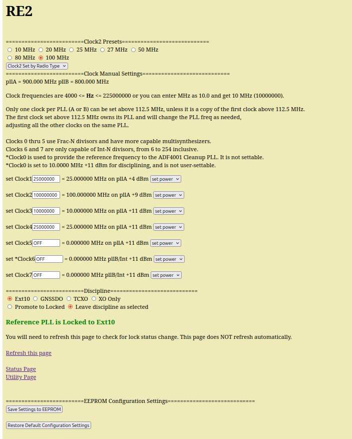
- WiFi web Interface - works with Windows, Apple or Linux systems.
- Common SDR and HF transceiver Frequency presets
-
Connections:
- SMA: GNSS Antenna
- External 10 MHz reference
- Seven SMA:User Selectable outputs 4 kHz to 225* MHz
- 2.1mm power barrel connector
- Four-layer, through-hole plated, silk-screen printed PCBs
- Aluminum enclosure
Example Web Interface
|
||||
Item Description |
Provider |
Source Code |
Notes |
Approximate Material Cost(excludes setup fees and shipping) |
Assembled RE2 PCBand Front&Rear Panels |
A newer,
not-yet-fabricated-and-tested version is now available as KiCad
files. Use the 'Production' sub-directory to obtain .zip
(Gerber), .bom and position.csv files for JLCPCB
fabrication.
|
US$40 | ||
| 2 x 20p CPU socket |
ADAFruit |
US$1 | ||
38x88x120mm Clam Shell Enclosure &Front/Rear Panels |
JLC |
|
Other sources possible. Enclosure needs to accept 84mm wide PCB. | US$3 & US$2 |
CPU |
||||
| RPI Pico 2W Arduino code |
RPI
Pico2W_with_header ReTr4_0_0916a_fllEngine_12_v2compile.zip |
code supports TR & OCXO option, not used for v2 |
US$8 + shipping |
|
Final
Assembly & Test
After receiving assembled PCB from fabrication and before final
assembly with the CPU & socket, first verify with an
ohmmeter that the power input line and the 5V and 3V regulator outputs
are not shorted. Next connect a current limited or low power source of
7-16 VDC power the board. Without CPU verify that there is only
a few mA flowing. The raw PCBs have already been pretested but doing
this makes sure nothing has gone wrong during component assembly or
soldering.
Final assembly and soldering of the CPU socket is next.
Plug a RPI Pico2W into the socket to assure allignment then mount
everything on the PCB squarely. Solder corner pins on the socket
making sure everything is flush and squarely aligned. Once the
position is good solder all the rest of the pin connections on both
the PCB and the CPU.
At this point again apply DC power and verify that there is 3.3V on
the LDO output and that the CPU comes alive. It should now be web
accessible.
You can now slide the PCB into the clam shell enclosure and attach
the end panels but leave the top clam shell off until later.
From here on you can use the Web page interface to set the DAC via
the utility page so that the on-board XO is preset correctly
Provide either a GNSS antenna or else a 10 MHz reference and
verify that when the corresponding disciplined mode is selected that
the unit shows LOCK when when using the Utility web page for
reporting.